

Czochralski process
Czochralski Process
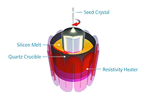
Today, a large portion of the silicon monocrystals are grown according to the Czochralski process,which involves melting polycrystalline high-purity silicon in a hyperpure quartz crucible and adding the dopant (usually B, P, As, Sb). A thin, monocrystalline seed crystal is dipped into the molten silicon. A large CZ crystal then develops from this thin crystal. Precise regulation of the molten
silicon temperature and flow, the crystal and crucible rotation, as well as the crystal pulling speed results in an extremely high-quality monocrystalline silicon ingot.
Cylindrical Grinding
Cylindrical Grinding
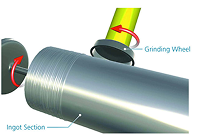
After segmenting and comprehensive quality control, the onocrystalline CZ or FZ silicon pieces are prepared for the wafering process. This means first precisely aligning the crystals, then cylindrical grinding of the ingot pieces to the required diameter. The final step is grinding orientation markings, such as notches for large-diameter wafers or straight edges (flats) on the side of small wafers.
Wire Slicing
Wire Slicing
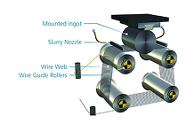
The first step when wafering the silicon ingots is multi-wire slicing, which is the slicing method commonly employed today. A very thin metal wire, which can be many miles long, is pulled over the wire guide rollers in such a way that a wire web with very precise spacing is spanned. Nozzles apply the slurry to the web while the silicon ingot is slowly pushed through the web. This technology makes it possible to slice complete silicon ingots into hundreds of silicon wafers in just one step. The individual process parameters must be carefully monitored in order to guarantee that the wafers are uniformly thick and that the two faces of each wafer are parallel to each another.
Edge Rounding
Edge Rounding
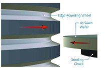
Monocrystalline silicon is a very brittle material with a high risk of breaking. Special care is consequently needed in order to avoid mechanical damages on the edge of the wafer.
The unrounded silicon wafer is mounted onto a grinding chuck and a profile rounding wheel rounds the edge of the wafer. The edge profile is rounded to match the customer specifications. Each wafer is optimized in order to avoid processing damages and maximize the yields in the component processes, such as CMP and lithography.
Laser marking
Laser marking
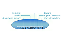
Laser marking is used to identify individual wafers or wafer batches in order to allow manufacturing traceability. Laser marking can take place in accordance with either industry standard or customer specifications. As a rule, the markings contain information on the wafer supplier, some technical information, and an individual wafer number.
Lapping
Lapping
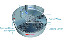
After the wafers have been sliced and the edges have been rounded, the wafers are lapped (or alternatively ground) in order to increase the parallelism of the silicon wafer surfaces and to remove any damage below the surface caused by the slicing process. For lapping, the silicon wafers are held in carrier wheels (lapping carriers) between the upper and lower lapping plates, which rotate in opposite directions. The addition of an abrasive (lapping slurry) helps remove roughly ten micrometers of silicon from each wafer surface.
Cleaning And Etching
Cleaning And Etching
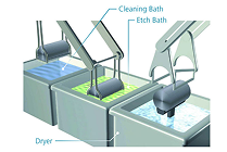
After the mechanical wafer processing, the silicon wafers are cleaned and etched in order to eliminate any remaining mechanical damage. Alkaline solutions, acids, or a combination of the two can be used for the etching.
Polishing
Polishing
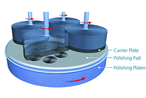
Polishing makes the silicon wafer surface smooth as glass and further improves the flatness. Wafers with a diameter of 200mm or less are usually polished on one side. The wafers are mounted on support plates and pressed against a polishing cloth that lies on a polishing plate. Wafers with a diameter of 300mm are polished on both sides. Like in the lapping process, the wafers are held by plates and simultaneously polished on the front and back by upper and lower polishing plates. The polishing agent (polishing slurry) and the pressure scheme determine the finished wafer’s surface quality and flatness.
Epitaxy
Epitaxy
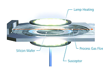
Applications with the toughest requirements call for silicon wafers with an especially high surface quality. In these cases, a thin, defect-free crystal layer is additionally deposited onto the polished surface from the gas phase. To apply the epitaxial layer, the silicon wafer is fastened to a susceptor and heated to a high temperature with the help of infrared lamps. The process gas flow and temperature are carefully controlled in order to create an epitaxial layer with a very homogeneous resistance and thickness profile.